- 您现在的位置:买卖IC网 > Sheet目录341 > MAX8791GTA+ (Maxim Integrated)IC MOSFET DRIVER 8-TQFN
�� �
�
�Single-Phase,� Synchronous� MOSFET� Drivers�
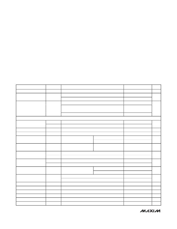
�ABSOLUTE� MAXIMUM� RATINGS�
�V� DD� to� GND...............…………………….…………..� -0.3V� to� +6V�
�SKIP� to� GND..................………………………………-0.3V� to� +6V�
�PWM� to� GND� ................……………………………….-0.3V� to� +6V�
�DL� to� GND� ..................................................-0.3V� to� (V� DD� +� 0.3V)�
�BST� to� GND� ............................................................-0.3V� to� +36V�
�DH� to� LX� ....................................................-0.3V� to� (V� BST� +� 0.3V)�
�BST� to� V� DD� .............................................................-0.3V� to� +30V�
�BST� to� LX� ................…………………………………...-0.3V� to� +6V�
�Continuous� Power� Dissipation� (T� A� =� +70°C)�
�8-Pin� 3mm� x� 3mm� TQFN�
�(derate� 23.8mW/°C� above� +70°C)� .............................1904mW�
�Operating� Temperature� Range� .........................-40°C� to� +105°C�
�Junction� Temperature� ......................................................+150°C�
�Storage� Temperature� Range� .............................-65°C� to� +150°C�
�Lead� Temperature� (soldering,� 10s)� .................................+300°C�
�Soldering� Temperature� (reflow)� .......................................+260°C�
�Stresses� beyond� those� listed� under� “Absolute� Maximum� Ratings”� may� cause� permanent� damage� to� the� device.� These� are� stress� ratings� only,� and� functional�
�operation� of� the� device� at� these� or� any� other� conditions� beyond� those� indicated� in� the� operational� sections� of� the� specifications� is� not� implied.� Exposure� to�
�absolute� maximum� rating� conditions� for� extended� periods� may� affect� device� reliability.�
�ELECTRICAL� CHARACTERISTICS�
�(Circuit� of� Figure� 1,� V� DD� =� V� SKIP� =� 5V,� T� A� =� -40� °� C� to� +105� °� C,� unless� otherwise� noted.� Typical� values� are� at� T� A� =� +25� °� C.)� (Note� 1)�
�PARAMETER�
�Input� Voltage� Range�
�V� DD� Undervoltage�
�Lockout� Threshold�
�SYMBOL�
�V� DD�
�V� UVLO(VDD)�
�CONDITIONS�
�Rising� edge,� PWM� disabled� below� this� level�
�Falling� edge,� PWM� disabled� below� this� level�
�MIN�
�4.20�
�3.0�
�TYP�
�3.7�
�3.5�
�MAX�
�5.50�
�4.0�
�UNITS�
�V�
�V�
�PWM� =� open;� after� the� shutdown� hold� time� has� expired�
�0.08�
�0.2�
�Quiescent� Supply�
�Current� (V� DD� )�
�I� DD�
�SKIP� =� GND,� PWM� =� GND,�
�LX� =� GND� (after� zero� crossing)�
�0.25�
�0.5�
�mA�
�DRIVERS�
�SKIP� =� GND� or� V� DD� ,� PWM� =� V� DD� ,� V� BST� =� 5V�
�0.6�
�1.5�
�PWM� Pulse� Width�
�DL� Propagation� Delay�
�DH� Propagation� Delay�
�t� ON(MIN)�
�t� OFF(MIN)�
�t� PWM-DL�
�t� PWM-DH�
�Minimum� on-time�
�Minimum� off-time�
�PWM� high� to� DL� low�
�PWM� low� to� DH� low�
�50�
�300�
�10�
�14�
�ns�
�ns�
�ns�
�DL-to-DH� Dead� Time�
�DH-to-DL� Dead� Time�
�DL� Transition� Time�
�DH� Transition� Time�
�t� DL-DH�
�t� DH-DL�
�t� F_DL�
�t� R_DL�
�t� F_DH�
�t� R_DH�
�DL� falling� to� DH� rising�
�DH� falling� to� DL� rising�
�Falling,� 3.0nF� load�
�Rising,� 3.0nF� load�
�Falling,� 3.0nF� load�
�Rising,� 3.0nF� load�
�T� A� =� 0°C� to� +85°C�
�T� A� =� -40°C� to� +105°C�
�T� A� =� 0°C� to� +85°C�
�T� A� =� -40°C� to� +105°C�
�15�
�15�
�15�
�15�
�30�
�30�
�12�
�14�
�8�
�10�
�ns�
�ns�
�ns�
�ns�
�DH� Driver� On-Resistance�
�DL� Driver� On-Resistance�
�R� ON(DH)�
�R� ON(DL)�
�BST-LX� forced� to� 5V�
�DL,� high� state� (pullup)�
�DL,� low� state� (pulldown)�
�DH,� high� state� (pullup)�
�DH,� low� state� (pulldown)�
�0.9�
�0.7�
�0.7�
�0.5�
�2.5�
�2.3�
�1.8�
�1.2�
�?�
�?�
�DH� Driver� Source� Current�
�I� DH_SOURCE� DH� forced� to� 2.5V,� BST� -� LX� forced� to� 5V�
�2.2�
�A�
�DH� Driver� Sink� Current�
�I� DH_SINK�
�DH� forced� to� 2.5V,� BST� -� LX� forced� to� 5V�
�2.7�
�A�
�DL� Driver� Source� Current� I� DL_SOURCE� DL� forced� to� 2.5V�
�2.7�
�A�
�DL� Driver� Sink� Current�
�Zero-Crossing� Threshold�
�I� DL_SINK�
�V� ZX�
�DL� forced� to� 2.5V�
�GND� -� LX,� SKIP� =� GND�
�8�
�3�
�A�
�mV�
�Boost� On-Resistance�
�R� ON(BST)�
�V� DD� =� 5V,� DH� =� LX� =� GND� (pulldown� state),� I� BST� =� 10mA�
�5�
�12�
�?�
�2�
�_______________________________________________________________________________________�
�发布紧急采购,3分钟左右您将得到回复。
相关PDF资料
MAX8811EEE+
IC DRVR DL PHASE HS 16-QSOP
MAX8821ETI+
IC LED DRVR WHITE BCKLGT 28-TQFN
MAX8822ETE+T
IC LED DRVR WHITE BCKLGT 16-TQFN
MAX8830EWE+T
IC LED DRVR WHITE BCKLGT 16-UCSP
MAX8831EWE+T
IC LED DRIVR WHITE BCKLGT 16-WLP
MAX8834ZEWP+T
IC LED DRIVR BCKLGT FLASH 20-WLP
MAX8855EVKIT+
KIT EVAL FOR MAX8855
MAX8879ETG+T
IC LED DRVR WT/RGB BCKLGT 24TQFN
相关代理商/技术参数
MAX8791GTA+T
功能描述:功率驱动器IC Single-Phase Synch MOSFET Driver RoHS:否 制造商:Micrel 产品:MOSFET Gate Drivers 类型:Low Cost High or Low Side MOSFET Driver 上升时间: 下降时间: 电源电压-最大:30 V 电源电压-最小:2.75 V 电源电流: 最大功率耗散: 最大工作温度:+ 85 C 安装风格:SMD/SMT 封装 / 箱体:SOIC-8 封装:Tube
MAX8792ETD+
制造商:Maxim Integrated Products 功能描述:SOFT SW PWM CNTRLR 1-OUT PWM CNTRLR 600KHZ 14TDFN EP - Rail/Tube 制造商:Maxim Integrated Products 功能描述:SINGLE QUICK- PWM STEP DOWN CONTROL
MAX8792ETD+T
功能描述:电压模式 PWM 控制器 Single Quick-PWM Step-Down Controller RoHS:否 制造商:Texas Instruments 输出端数量:1 拓扑结构:Buck 输出电压:34 V 输出电流: 开关频率: 工作电源电压:4.5 V to 5.5 V 电源电流:600 uA 最大工作温度:+ 125 C 最小工作温度:- 40 C 封装 / 箱体:WSON-8 封装:Reel
MAX8792EVKIT+
功能描述:电源管理IC开发工具 MAX8792 Eval Kit RoHS:否 制造商:Maxim Integrated 产品:Evaluation Kits 类型:Battery Management 工具用于评估:MAX17710GB 输入电压: 输出电压:1.8 V
MAX8794ETB/V+T
功能描述:低压差稳压器 - LDO Low-Voltage DDR Linear Regulator RoHS:否 制造商:Texas Instruments 最大输入电压:36 V 输出电压:1.4 V to 20.5 V 回动电压(最大值):307 mV 输出电流:1 A 负载调节:0.3 % 输出端数量: 输出类型:Fixed 最大工作温度:+ 125 C 安装风格:SMD/SMT 封装 / 箱体:VQFN-20
MAX8794ETB+
制造商:Maxim Integrated Products 功能描述: 制造商:Maxim Integrated Products 功能描述:LOW-VOLTAGE DDR LINEAR REGULATOR - Rail/Tube
MAX8794ETB+T
功能描述:低压差稳压器 - LDO Low-Voltage DDR Linear Regulator RoHS:否 制造商:Texas Instruments 最大输入电压:36 V 输出电压:1.4 V to 20.5 V 回动电压(最大值):307 mV 输出电流:1 A 负载调节:0.3 % 输出端数量: 输出类型:Fixed 最大工作温度:+ 125 C 安装风格:SMD/SMT 封装 / 箱体:VQFN-20
MAX8795AETJ+
功能描述:直流/直流开关转换器 TFT-LCD DC/DC Converter RoHS:否 制造商:STMicroelectronics 最大输入电压:4.5 V 开关频率:1.5 MHz 输出电压:4.6 V 输出电流:250 mA 输出端数量:2 最大工作温度:+ 85 C 安装风格:SMD/SMT